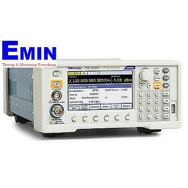
Máy phát tín hiệu vector RF Tektronix TEKTRONIX TSG4102A
Hãng sản xuất: TEKTRONIX Model: TSG4102A - Yêu cầu báo giá

- Yêu cầu báo giá
- Liên hệ
Tham khảo dịch vụ Hiệu chuẩn-Kiểm định và Sửa chữa
Gọi để có giá tốt
TP. Hà Nội: (024) 35.381.269
TP. Đà Nẵng: (023) 63.747.711
TP. Bắc Ninh: (0222)730.39.68
TP. HCM: (028) 38.119.636
Giải tần: 950 kHz đến 2.0 GHz
Độ phân giải tần số: 1 μHz
Tốc độ chuyển mạch: <8 ms
Giải công suất ra: +16.5 dBm to –110 dBm
Bộ dao động VCXO M01 (cấu hình lựa chọn) :
+ Độ chính xác ban đầu hiệu chuẩn : <±0.5 ppm, ở 20 phút tăng nhiệt, ở 18 ºC ~ 28 ºC
+ Độ già hóa : <±3.0 ppm/year
Bộ dao động VCXO M00 (Mua thêm phụ kiện M00) :
+ Độ chính xác ban đầu hiệu chuẩn : <±0.02 ppm, ở 20 phút tăng nhiệt, ở 18 ºC ~ 28 ºC
+ Độ già hóa : <±0.05 ppm/year
Kiểu điều chế Analog: AM, FM, ΦM, Pulse
Kiểu điều chế Vector: (ASK, FSK, PSK, QAM , CPM, VSB) đến 6Mhz (Mua thêm phụ kiện VM00)
Điều chế nguồn: Sine, ramp, saw, square, pulse, noise
Giao tiếp: Lan, GPIB, RS232, USB
Cung cấp kèm theo: 1m cáp RF (N-type to N-type), CD tài liệu, Dây nguồn
Chú ý : Đối với mỗi mô hình cơ bản, có 3 tùy chọn bắt buộc nhưng độc quyền cần chỉ định tại thời điểm đặt hàng M00, M01,E1
Option
Options M00 or M01 must be specified at the time of instrument order.
- M00 Instrument with oven-controlled crystal oscillator (OCXO)
- M01 Instrument with voltage-controlled crystal oscillator (VCXO)
- GPIB Adds GPIB interface
- TSG4100A-RM1 Single rack mount kit (can be ordered separately)
- TSG4100A-RM2 Dual rack mount kit (can be ordered separately)
- TSG4100A-ATT 30 dB, 5 W RF attenuator up to 6 GHz
- D1 A list of performance verification test results
Software options
To upgrade to vector/digital modulation capability and/or add more modulation options after initial purchase, order "TSG4100A-UP + VM xx” instead of “TSG410xA VMxx”.
- VM00 Basic vector modulation package with internal 6 MHz modulation bandwidth
- VM01 GSM modulation (requires Option VM00)
- VM02 GSM EDGE modulation (requires Option VM00)
- VM03 W-CDMA modulation (requires Option VM00)
- VM04 APCO-25 modulation (requires Option VM00)
- VM05 DECT modulation (requires Option VM00)
- VM06 NADC modulation (requires Option VM00)
- VM07 PDC modulation (requires Option VM00)
- VM08 TETRA modulation (requires Option VM00)
- VM10 Audio Clip (analog AM and FM)
- EIQ External 200 MHz modulation bandwidth (requires Option VM00)
- .................................................................................................................................................................
Specifications
All specifications apply to all models unless noted otherwise.
Frequency
- BNC output, all models
- DC to 62.5 MHz
- N-type outputs
-
- TSG4102A
- 950 kHz to 2.0 GHz
- TSG4104A
- 950 kHz to 4.0 GHz
- TSG4106A
- 950 kHz to 6.0 GHz
- Frequency resolution
- 1 μHz at any frequency
- Switching speed
- <8 ms="" to="" within="" 1="" ppm="" dd="">
- Frequency error
- <(10–18 + time-base error) × fc
- Frequency stability
- 1 × 10–11 (1 s Allan variance)
Front panel BNC output
- Frequency range
- DC to 62.5 MHz
- Amplitude
- 1.00 VRMS to 0.001 VRMS (-47 dBm to +14.96 dBm)
- Offset
- ±1.5 VDC
- Offset resolution
- 5 mV
- Maximum excursion
- 1.817 V (amplitude + offset)
- Amplitude resolution
- <1 dd="">
- Amplitude accuracy
- ±0.7 dB
- Harmonics, typical
- <–40 dBc
- Spurious, typical
- <–65 dBc
- Output coupling
- DC, 50 Ω ±2%
- Impedance
- 50 Ω
- Reverse protection
- ±5 VDC
- VSWR, typical
- < 1.6 :1
Front panel N-type output
- Power output
-
- TSG4102A
- +16.5 dBm to –110 dBm
- TSG4104A
- +16.5 dBm to –110 dBm (<3 ghz="" dd="">
- TSG4106A
- +16.5 dBm to –110 dBm (<4 ghz="" p="">+10 dBm to –110 dBm (4-6 GHz)
- Voltage output
-
- TSG4102A
- 1.5 VRMS to 0.7VRMS
- TSG4104A
- 1.5 VRMS to 0.7 μVRMS (<3 ghz="" dd="">
- TSG4106A
- 1.5 VRMS to 0.7 μVRMS (<4 ghz="" dd="">
- Amplitude resolution
- 0.01 dBm
- Amplitude accuracy
-
- CW, 50 Ω load (dB, typical)
- CW, 50 Ω load (dB, max)
- Impedance
- 50 Ω
- Output coupling
- AC, 50 Ω
- VSWR, typical
- <1.5 2="" mhz="" to="" 2="" ghz="" p=""><1.8 2="" ghz="" to="" 6="" ghz="" p="">
- Reverse protection
- 30 VDC, +25 dBm
- IQ modulation output level accuracy
- Output amplitude is -5 dBm.
Spectral purity of the RF output
- Subharmonics
- None
- Harmonics, maximum
- Output level <0 dbm="" 1="" ghz="" cw="" signal="" dl="">
- TSG4102A and TSG4104A
- < -38 dBc
- TSG4106A
- < -30 dBc
- Harmonics, typical (output level < 0 dBm)
- < -35 dBc, CW , Fc < 2 GHz
- Spurious (typical)
- Output level -10 dBm, CW
- < -68 dBc
- >10 kHz from carrier in 950 kHz to 1 GHz
- < -60 dBc
- >10 kHz from carrier in 1 GHz to 2 GHz
- < -55 dBc
- >10 kHz from carrier in 2 GHz to 4 GHz
- < -55 dBc
- >10 kHz from carrier in 4 GHz to 6 GHz
- Residual FM, typical
- 1 Hz rms (300 Hz to 3 kHz bandwidth)
- Residual AM, typical
- 0.006 % rms (300 Hz to 3 kHz bandwidth)
- SSB phase noise
- Output level is +5 dBm at 18 °C to 28 °C.
- SSB phase noise at 1 GHz carrier, maximum (output level +5 dBm, 5 ℃ to 40 ℃)
-
- 1 kHz offset
- –95 dBc/Hz
- 10 kHz offset
- –106 dBc/Hz
- 20 kHz offset
- –107 dBc/Hz
- 1 MHz offset
- –120 dBc/Hz
- 2 GHz offset
- –118 dBc/Hz
- >3 GHz offset
- –120 dBc/Hz
-
-


Phase setting (front panel outputs)
- Maximum phase step
- ±360º
- Phase resolution
- 0.01º (DC to 100 MHz)
0.1º (100 MHz to 1 GHz)
1.0º (1 GHz to 6 GHz)
OCXO time-base (Option M00 or Option E1)
- Oscillator type
- Oven-controlled, 3rd OT, SC-cut crystal
- Initial accuracy at calibration (20 minute warm-up, at 18 ºC to 28 ºC)
- <±0.02 ppm
- Temperature drift (0 ºC to 40 ºC)
- <±0.003 ppm
- Aging
- <±0.05 ppm/year
VCXO time base (Option M01)
- Initial accuracy at calibration (20 minute warm-up, at 18 ºC to 28 ºC)
- <±0.5 ppm
- Temperature drift (0 ºC to 40 ºC)
- <±5.0 ppm
- Aging
- <±3.0 ppm/year
Time-base input
- Frequency
- 10 MHz, ±2 ppm
- Amplitude
- 0.5 VP-P to 4 VP-P (–2 dBm to +16 dBm)
- Input impedance
- 50 Ω, AC coupled
Time-base output
- Frequency
- 10 MHz, sine
- Source
- 50 Ω, DC transformer coupled
- Amplitude
- >7.5 dBm
Internal modulation source
- Waveforms
- Sine, ramp, saw, square, pulse, noise
- Sine THD
- –74 dBc (typical at 20 kHz)
- Ramp linearity
- <0.05 1="" khz="" dd="">
- Rate
-
- TSG4102A and TSG4104A
- 1 μHz to 500 kHz: < 62.5 MHz CF
1 μHz to 50 kHz: ≥62.5 MHz
- TSG4106A
- 1 μHz to 500 kHz: < 93.75 MHz CF
1 μHz to 50 kHz: ≥93.75 MHz
- Rate resolution
- 1 μHz
- Rate error
- 1:231 + time-base error
- Noise function
- White Gaussian noise (rms = dev / 5)
- Noise bandwidth
- 1 μHz < ENBW < 50 kHz
- Pulse generator period
- 1 μs to 10 s
- Pulse generator width
- 100 ns to 9999.9999 ms
- Pulse timing resolution
- 5 ns
- Pulse noise function
- Length 2N-1 PRBS 5 ≤ N ≤ 32, bit period 100 nS to 10 S
Analog modulation output
- Connector type
- BNC (rear panel)
- Impedance
- 50 Ω
- Function
- AM, FM, ΦM, Pulse
- Scale factor
- ±1 V for ± full deviation
- Pulse/Blank
- Low = 0 V
Hi = 3.3 V
External analog modulation input
- Connector type
- BNC (rear panel)
- Impedance
- 100 kΩ
- Function
- AM, FM, ΦM, Pulse
- Scale factor
- ±1 V for ± full deviation
- Pulse/Blank
- Low = 0 V
Hi = 3.3 V
- Input coupling
- DC or 4 Hz High-pass
- Pulse Threshold
- +1 VDC
- Input Offset
- < 500 μV
Amplitude modulation
- Range
- 0 to 100% (decreases above +7 dBm)
- Resolution
- 0.1%
- Modulation source
- Internal or external
- Modulation distortion, typical
-
- BNC output
- <1 fc="" 62="" 5="" mhz="" fm="1" khz="" dd="">
- N-type output
- <3 fc=""> 62.5 MHz, fm = 1 kHz)
- Modulation bandwidth (external)
- >100 kHz
Frequency modulation
- Minimum frequency deviation
- 0.01 Hz
- Maximum frequency deviation
-
- TSG4102A and TSG4104A
- Smaller of fc and 64 MHz – fc. In 0 to 62.5 MHz
- TSG4106A
- Smaller of fc and 96 MHz – fc. In 0 to 93.75 MHz
- Deviation resolution
- 0.1 Hz
- Deviation accuracy, typical
-
- TSG4102A and TSG4104A
- < 0.1% of selected deviation + 5 Hz (fc < 62.5 MHz)
< 2% of selected deviation + 20 Hz (fc > 62.5 MHz)
- TSG4106A
- < 0.1% of selected deviation + 5 Hz (fc < 93.75 MHz)
< 2% of selected deviation + 20 Hz (fc > 93.75 MHz)
- Modulation source
- Internal or external
- Modulation distortion, typical
- < -60 dB (fc=100 MHz, fm=1 KHz, fd= 3 KHz)
- External FM carrier offset, typical
- < ±0.001 X FM deviation
- Modulation bandwidth, typical
-
- TSG4102A and TSG4104A
- 500 kHz (fc < 62.5 MHz)
100 kHz (fc > 62.5 MHz)
- TSG4106A
- 500 kHz (fc < 93.75 MHz)
100 kHz (fc > 93.75 MHz)
Phase modulation
- Deviation
- 0º to 360º
- Deviation resolution, typical
- 0.01º (DC to 100 MHz)
0.1º (100 MHz to 1 GHz)
1º (1 GHz and above)
- Deviation accuracy, typical
-
- TSG4102A and TSG4104A
- 2% (fc < 62.5 MHz)
3% (fc > 62.5 MHz)
- TSG4106A
- 2% (fc < 93.75 MHz)
3% (fc > 93.75 MHz)
- Modulation source
- Internal or external
- Modulation distortion, typical
- < -60 dB (fc = 100 MHz, fm =1 kHz, ΦD = 50º)
- Modulation bandwidth, typical
-
- TSG4102A and TSG4104A
- 500 kHz (fc < 62.5 MHz)
100 kHz (fc > 62.5 MHz)
- TSG4106A
- 500 kHz (fc < 93.75 MHz)
100 kHz (fc > 93.75 MHz)
Pulse modulation
- Pulse mode
- Logic High turns RF output ON
- On-Off ratio, typical
-
- BNC output
- > 70 dB
- Type-N output
- > 57 dB (fc < 1.0 GHz)
> 40 dB (1.0 GHz ≤ fc < 4.0 GHz)
> 35 dB (4.0 GHz ≤ fc < 6.0 GHz)
- Pulse feed-through, typical
- 10% of carrier for 20 ns at turn on
- Turn On-Off delay
- 60 ns
- RF Rise-Fall time, typical
- 20 ns
- Modulation source
- Internal or external pulse
Interface connectors
- USB
- USB 2.0, host
- Ethernet (LAN)
- 10/100 Base-T.TCP/IP and DHCP default
- GPIB
- IEEE488.2
- RS-232
- 4800 to 115,200 baud, RTS/CTS flow
External I/Q modulation (Option EIQ)
- Carrier frequency range
- 400 MHz to 2.0 GHz (TSG4102A)
400 MHz to 4.0 GHz (TSG4104A)
400 MHz to 6.0 GHz (TSG4106A)
- I/Q inputs (rear panel)
- 50 Ω, ±0.5 V
- I/Q full scale input
- (I2 + Q2)1/2 = 0.5 V
- Modulation bandwidth
- max 400 MHz RF bandwidth
- I or Q input offset
- <500 v="" dd="">
- Carrier suppression
- > -45 dBc for fc ≤ 3 GHz
> -40 dBc for 3 GHz < fc ≤ 5 GHz
> -35 dBc for fc > 5 GHz
- I and Q baseband modulation bandwidth (3 dB from fc)
- > 200 MHz (fc < 2.5 GHz, RF BW >400 MHz)
> 150 MHz (fc > 2.5 GHz, RF BW >300 MHz)
Dual baseband generator (Option VM00)
- Channels
- 2 (I and Q)
- DAC data format
- Dual 14-bit at 125 MS/s
- Reconstruction filter
- 10 MHz, 3rd order Bessel LPF
- Arbitrary symbol memory
- Up to 16 Mbits
- Symbol rate
- 1 Hz to 6 MHz (1 μHz resolution)
- Symbol length
- 1 to 9 bits (maps to constellation)
- Symbol mapping
- Default or user-defined constellation
- Symbol source (User-defined symbols, built-in PRBS generator, or settable pattern generator)
-
- PRBS length
- 2n – 1 (5 < n < 32; 31 to about 4.3 × 10⁹ symbols)
- Pattern generator
- 16 bits
- Digital filtering
-
- Filter type
- Raised Cosine, Root Raised Cosine, Gaussian, Rectangular, Linear, Sinc, linearized Gaussian, C4FM, customized FIR
- Filter length
- 24 symbols
- Noise impairments
-
- Additive noise
- White, Gaussian
- Level
- –70 dBc to –10 dBc
Basic vector modulation formats (Option VM00)
- Formats by bit
- Others
- OQPSK, DQPSK, π/4DQPSK, 3π/8 8 PSK
Digital modulation applications (typical)
- Digital modulation applications options
-
Option VM01 GSM, (GMSK, 270.833 kS/s, 935 MHz, 0 dBm), RMS EVM: 0.6%

Option VM02 GSM-EDGE, (3π/8 8PSK, 270.833 kS/s, 935 MHz, 0 dBm), RMS EVM: 0.30%

Option VM03 W-CDMA, (QPSK,3.840Mcps, 2.1425GHz, 0dBm), RMS EVM: 1.7%


Option VM03 W-CDMA (QPSK,3.840Mcps, 1.85 GHz, 0dBm), RMS EVM: 1.7%


Option VM04 APCO-25, (4FSK-C4FM, 4.8 kS/s,850 MHz, 0 dBm), Freq Err: 0.5%

Option VM05 DECT, (2FSK 1.152 Mbps,1.925 GHz, 0 dBm), RMS FSK Err: 1.5%

Option VM06 NADC, (π/4 DQPSK, 24.3 kS/s, 875 MHz, 0 dBm), RMS EVM: 0.3%

Option VM07 PDC, (π/4 DQPSK, 21 kS/s, 800 MHz, 0 dBm), RMS EVM: 0.6%

Option VM08 TETRA, (π/4 DQPSK,18 kS/s, 420 MHz, 0 dBm), RMS EVM: 0.7%

32QAM, (6 MS/s, 5.8 GHz, Root raised cosine filter, 0 dBm), RMS EVM: 1.6%

256QAM, (6 MS/s, 2.45 GHz, Root raised cosine filter, 0 dBm), RMS EVM: 1.1%


TSG4100A-ATT Option
- Nominal impedance
- 50 Ω
- Nominal attenuation
- 30 dB
- Frequency range
- DC to 6 GHz
- Attenuation deviation
- ±0.75 dB (DC to 6 GHz)
- Maximum VSWR
- 1.15 (DC to 4 GHz)
1.2 (4 GHz to 6 GHz)
- Power rating
- 5 Watt average power up to 25 ˚C ambient temperature, linearly derated to 1 Watt at 125 ˚C ambient temperature.
- Weight
- 0.052 kg
- Operating temperature
- -65 °C to 125 °C
- Compliance
- 2011/65/EU (RoHS) compliant
Rear-panel markers
- Type
- Symbol Clock, Data Frame, TDMA, and user-defined
- Amplitude
- 0.5 to 4 Vpp (–2 dBm to +16 dBm)
- Output impedance
- 50 Ω, AC coupled
Physical characteristics
- Dimensions
-
- Height
- 114 mm (4.5 in)
- Width
- 216 mm (8.5 in)
- Depth
- 347 mm (13.7 in)
- Weight
- 5.4 kg (12 lbs)
Operating characteristics
- Temperature
-
- Operating
- +5 °C to +40 °C
- Non-operating
- -20 °C to +60 °C
- Humidity
- Altitude
-
- Operating
- Up to 3,000 m
- Non-operating
- Up to 12,000 m
- Line power
- <90 w="" 90="" to="" 264="" vac="" 47="" to="" 63="" hz="" with="" pfc="" dd="">
- Vibration and shock
-
- Random vibration
- Mechanical shock
Regulatory information
- EC Declaration of Conformity - EMC
-
- EMC Directive 2004/108/EC
- EN 61326-1
- Radiated and Conducted emissions
- Class A
- Australia/New Zealand
- Australia Radio Communications Act 1992
- Korea
- KCC
- Safety
-
- Third Party Certification Standards
- UL 61010; CSA C22.2 No. 61010-1
- EC Declaration of Conformity - Low Voltage
- Low Voltage Directive 2006/95/EC; EN61010-1
- Safety Certification Compliance
- Cam kết chất lượng
- Bảo hành chính hãng
- Giao hàng tận nơi
- Đơn giản hóa giao dịch